Introduction
Flexible PCBs (Printed Circuit Boards) are revolutionizing modern electronics, making devices smaller and more durable. As the need for compact, high-performance electronics grows, understanding their manufacturing process becomes essential. In this guide, you will learn every step of flexible PCB production, from design to final assembly, ensuring you master the techniques needed for high-quality flexible circuits.
What Are Flexible PCBs and Why Are They Important?
Definition of Flexible PCBs
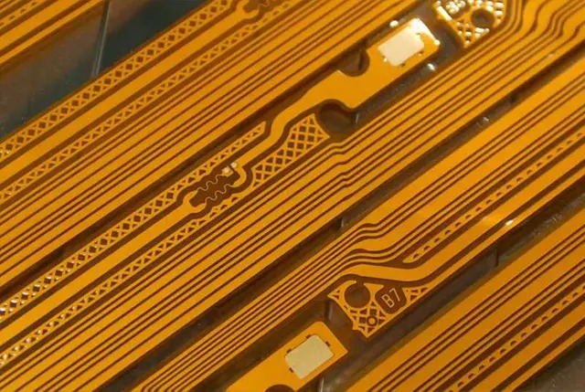
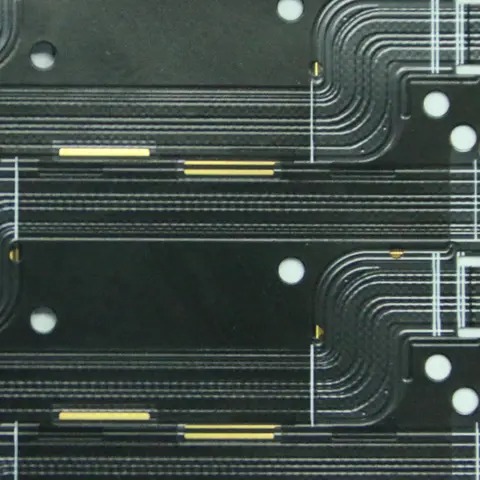
Flexible PCBs, often referred to as flex circuits, are a type of PCB made from flexible materials like polyimide or polyester. These boards can bend, twist, and fold without breaking, unlike traditional rigid PCBs. The flexibility allows for more innovative designs, especially in compact electronics where space is a premium. Flexible PCBs are commonly used in smartphones, wearable devices, and medical equipment.
Applications of Flexible PCBs
Flexible PCBs play a crucial role across various industries, particularly in applications that require space-saving, lightweight, and durable solutions. The following table breaks down the applications of flexible PCBs in wearable tech, automotive, aerospace, and medical devices, along with the technical specifications and key considerations for each industry.
| Application Area | Technical Parameters | Physical Properties | Considerations | Applicable Scope |
| Wearable Tech | Functionality: Heart rate monitoring, activity tracking | Minimum bend radius: 2mm; Operating temperature: -40°C to +85°C | Ensure signal stability and sensor accuracy after prolonged bending | Fitness trackers, smartwatches, health monitoring devices |
| Automotive Electronics | Functionality: Sensors, battery management | Mechanical strength: 80-120 MPa; Thermal resistance: up to 200°C | Maintain reliability in extreme temperature and vibration environments | Automotive sensors, dashboards, battery management systems |
| Aerospace | Functionality: Aerospace components, high-frequency signal transmission | Coefficient of thermal expansion: 10-20 ppm/°C; Operating temperature: -50°C to +200°C | Ensure long-term durability and signal stability in high-frequency applications | Aerospace sensors, high-performance communication equipment |
| Medical Devices | Functionality: Implants, diagnostic instruments | Flexural endurance: >100,000 cycles; Corrosion resistance: >99% | Material choice must ensure biocompatibility and environmental resistance | Medical sensors, pacemakers, diagnostic equipment |
Tip:When selecting flexible PCBs for medical and aerospace applications, it's essential to focus on material biocompatibility and thermal resistance to ensure device reliability and patient safety.
Advantages of Flexible PCBs
Flexible PCBs offer several benefits, including significant space and weight savings. They eliminate the need for additional connectors and cables, reducing up to 60% of the board's size and weight. Additionally, they are durable and can withstand bending and dynamic movements, making them ideal for applications like wearables. The ability to conform to 3D shapes also allows for innovative designs in tight spaces.

Overview of the Flexible PCB Manufacturing Process
Initial Considerations: Design and Layout
Designing a flexible PCB starts with understanding the specific requirements for flexibility and functionality. A well-thought-out design ensures the circuit can handle stress points, avoid flex failures, and meet performance standards. Design software like Altium Designer or Cadence Allegro is commonly used to create the circuit blueprint, which is then converted into Gerber files for manufacturing.
Material Selection for Flex Circuits
Selecting the right materials is crucial for flexible PCBs. The table below compares common flexible PCB materials such as Polyimide (PI) and Polyester (PET), outlining the technical specifications, applications, and considerations for each.
| Material | Polyimide (PI) | Polyester (PET) | Copper Foil (Conductive Layer) |
| Thermal Stability | Excellent thermal resistance, up to 260°C | Moderate thermal resistance, up to 150°C | High thermal conductivity, suitable for heat dissipation |
| Flexibility | Highly flexible, ideal for dynamic applications | Moderate flexibility, less durable | Flexible when bonded to substrate for signal transmission |
| Mechanical Strength | High tensile strength (up to 120 MPa) | Lower tensile strength (around 60 MPa) | Supports circuit integrity and flexibility |
| Corrosion Resistance | Excellent, high resistance to environmental factors | Good, but less resistant to harsh chemicals | Corrosion-resistant coatings (ENIG, HASL) protect copper |
| Cost | Higher cost due to advanced properties | Cost-effective, suitable for less demanding applications | Dependent on coating, with ENIG being more expensive than HASL |
| Common Applications | Aerospace, medical devices, wearables | Budget-friendly applications, consumer electronics | Found in all flexible PCBs for electrical pathways |
| Considerations | Requires precise processing and high manufacturing standards | Limited durability in harsh environments | Proper bonding to substrate is critical for electrical reliability |
Lamination and Layer Bonding Techniques
Lamination is the process of bonding layers of copper foil to the flexible substrate, using heat and pressure to create a robust structure. In more advanced designs, adhesive-less bonding techniques are used, which improve flexibility by eliminating adhesives that can create rigidity. Precise temperature and pressure control are critical to ensuring a high-quality, flexible circuit board.
Flexible PCB Design Considerations
Mechanical Stress Management
Designing a flexible PCB requires careful attention to mechanical stress points, especially at locations where the board will bend. Components should be placed away from areas that will be subject to bending to avoid damage. Using flexible materials like polyimide helps manage stress, but careful routing and trace design are also necessary to prevent failure due to flexing.
Trace Design for Flexibility and Integrity
The design of traces on flexible PCBs is crucial to ensure signal integrity and flexibility. Narrow traces are often necessary for high-density designs, but care must be taken to ensure they can withstand the mechanical stress caused by bending. To enhance flexibility, traces can be routed in serpentine patterns or meanders, allowing the circuit to flex without cracking.
Simulation and Prototyping Tools
Before manufacturing, simulations are vital to verify the design’s integrity, especially when it comes to the mechanical stress and flexing behavior of the PCB. CAD tools offer features like bend radius simulation and dynamic testing to predict how the board will behave in real-world applications. Prototyping helps to identify potential issues before the final manufacturing stage.
Step-by-Step Guide to Flexible PCB Manufacturing
Step 1: Design and Layout Creation
Creating an optimal design is crucial for flexible PCBs, as it directly influences performance and reliability. The design must account for the unique bending characteristics of flexible materials, such as defining the bend radius to prevent trace cracks. CAD tools like Altium Designer and Cadence Allegro incorporate automated design rule checks (DRC), ensuring that trace widths, component placements, and spacing adhere to mechanical and electrical constraints. Simulation tools also allow designers to test bend stress before manufacturing to avoid potential failures.
Step 2: Material Selection
Selecting the right material is vital for ensuring the flexible PCB's durability and performance. Polyimide (PI) is commonly used for its excellent thermal stability and mechanical strength, ideal for applications requiring frequent flexing. For cost-sensitive applications, polyester (PET) may be chosen due to its lower price but reduced heat resistance. Advanced materials, like Liquid Crystal Polymer (LCP), are utilized for high-frequency circuits due to their low dielectric constant and high thermal performance. Material selection must consider factors like operating temperature, mechanical stress, and electrical performance.
Step 3: Lamination and Layer Bonding
The lamination process is key to achieving a flexible and durable PCB. During this phase, copper foil is bonded to the flexible substrate under controlled heat and pressure, ensuring the copper adheres properly. For multi-layer flexible PCBs, precision in bonding multiple layers is critical, as misalignment can result in signal loss or mechanical stress at the interface. Adhesive-less bonding techniques, such as direct copper bonding (DCB), offer thinner and more flexible designs, enhancing the PCB's resistance to mechanical fatigue over time.
Step 4: Circuit Patterning and Etching
In flexible PCB manufacturing, circuit patterning involves photolithography, where a photoresist layer is applied to the copper. UV light then hardens the exposed areas based on the design. This process requires precision to ensure trace widths and spacing meet the required electrical standards. The subsequent etching removes unprotected copper, leaving the desired circuit pattern. The etching process uses specialized chemicals that ensure fine details are maintained without damaging the substrate, crucial for high-density, flexible designs used in compact electronics.
Step 5: Drilling and Via Formation
For multi-layer flexible PCBs, vias are necessary to establish connections between layers. Laser drilling, with its high precision, is preferred for flexible circuits to create small vias (as narrow as 25 micrometers), essential for high-density designs. The process must be executed with care to avoid damaging the delicate substrate. The holes are plated with copper to form electrical paths between the layers. Accurate via formation is critical for ensuring signal integrity, as improperly drilled vias can result in signal loss or weak mechanical bonding between layers.
Step 6: Copper Plating and Surface Finishing
Copper plating is a critical step for ensuring proper conductivity in flexible PCBs. The electroplating process adds a thin layer of copper to vias and traces, providing reliable electrical connections. The surface finish, such as Electroless Nickel Immersion Gold (ENIG), is applied to prevent copper oxidation, which could hinder electrical performance and solderability. The choice of finish affects the board's ability to withstand mechanical stress and environmental exposure, which is crucial for devices that require high durability, such as wearables or automotive electronics.
Step 7: Coverlay Application
A coverlay is applied to flexible PCBs to protect the conductive layers while maintaining the board's flexibility. Made typically of polyimide, the coverlay shields the PCB from environmental factors such as moisture, dust, and chemicals. Precision is crucial during this stage to ensure that key connection points and components remain exposed. Improper alignment of the coverlay can lead to open circuits or poor solder connections, affecting the PCB’s performance. This protective layer also plays a role in the PCB’s ability to endure repeated bending without cracking.
Step 8: Cutting and Profiling
After the PCB is fully formed, the final shape is achieved through cutting and profiling. Laser cutting is the preferred method for flexible PCBs, as it offers high precision without introducing stress to the material. This method ensures clean cuts and avoids warping that could occur with mechanical cutting tools. The cutting process must account for tight tolerances to ensure the flexible PCB fits perfectly within its final product, such as wearable devices or compact sensors, where space constraints are critical.
Step 9: Testing and Quality Assurance
Each flexible PCB undergoes rigorous testing to ensure it meets all required specifications. Electrical continuity and impedance testing ensure that signals flow correctly and that there are no short circuits. Flex cycle testing is particularly important, simulating thousands of bending cycles to ensure that the PCB can withstand mechanical stress over time without failure. Other tests, like thermal cycling and environmental resistance testing, validate the PCB’s ability to perform in harsh conditions, crucial for industries such as aerospace and medical devices, where reliability is paramount.
Step 10: Final Assembly and Integration
In the final stage, components are assembled onto the flexible PCB using surface-mount technology (SMT). Due to the compact nature of flexible PCBs, components are often placed in tight spaces, requiring precise alignment. The PCB is then integrated into its final product, such as a wearable device or automotive sensor. Careful handling during this stage is crucial to avoid introducing mechanical stress that could lead to failure. The integration process also involves testing to ensure that the flexible PCB operates correctly within the final product's environment, whether it’s a flexible display or a medical sensor.

Benefits of Flexible PCBs in Modern Applications
Space and Weight Savings
Flexible PCBs enable dramatic reductions in both size and weight by eliminating bulky connectors, cables, and rigid components. Their ability to bend and conform to the contours of devices reduces the need for additional structural components, saving up to 60% in space. This capability is particularly beneficial in compact, portable applications, such as wearables, smartphones, and medical implants, where every millimeter and gram counts. As electronic devices become smaller and more portable, flexible PCBs are essential for maintaining high functionality without sacrificing design efficiency.
Durability and Flexibility
The following table provides a detailed breakdown of the durability and flexibility of flexible PCBs in dynamic environments, offering essential technical parameters, application guidelines, and considerations. It helps understand how flexible PCBs perform under extreme conditions in various applications.
Flexible PCB Durability and Flexibility Applications and Technical Specifications
| Application Area | Technical Parameters | Physical Properties | Considerations | Applicable Scope |
| Bending Durability | Bend cycles: >200,000 | Minimum bend radius: 2mm-6mm | Avoid placing critical components in frequent bending areas | Wearables, portable electronics, automotive |
| Mechanical Stress Resistance | Yield strength: 120 MPa | Tensile strength: 80-100 MPa | Avoid excessive stretching and compression during design | Dynamic environments, sensors, automotive electronics |
| Thermal Stability | Maximum thermal stability: up to 260°C | Coefficient of thermal expansion (CTE): 20-50 ppm/°C | Choose high thermal stability materials for high-temperature environments | Automotive, industrial applications |
| Corrosion Resistance | Post-corrosion failure cycle: >100,000 | Moisture absorption rate: <0.5% | Keep dry, perform moisture protection during use | Medical devices, automotive electronics |
| Flexural Strength | Elongation at break: >100% | Adhesive layer thickness: 0.002-0.005 inches | Ensure compatibility between bending and materials | Wearable electronics, portable devices |
| Coverlay Strength | Coverlay material thickness: 0.001-0.002 inches | Adhesion strength: >2N/mm | Precise coverlay alignment to avoid covering connection points | Medical sensors, wearable devices |
Design Freedom and Innovation
Flexible PCBs provide unparalleled design freedom, enabling new innovations in electronics. Their ability to be shaped and bent into 3D configurations allows designers to integrate circuits into unconventional, space-efficient forms. In fields like wearable electronics, this flexibility is crucial for creating products that comfortably fit the human body while maintaining high-performance standards. The ability to mold these circuits into compact, flexible formats opens new possibilities for product design, such as foldable displays and curved devices, which were previously impossible with rigid PCBs.
Conclusion
Flexible PCB manufacturing involves a multi-step process, from design and material selection to assembly and testing. It enables the creation of high-quality flexible PCBs tailored to modern needs, including applications in wearables, automotive components, and aerospace technology. HECTACH offers cutting-edge solutions for flexible PCBs, ensuring high durability and flexibility for devices that require space efficiency and robust performance. Their products provide unmatched value, catering to industries with demanding, high-performance requirements.
FAQ
Q: What is a Flexible PCB?
A: A flexible PCB (Printed Circuit Board) is a type of circuit board made from flexible materials like polyimide, allowing it to bend and twist. It's used in devices requiring compact, lightweight designs, such as wearables and medical devices.
Q: Why are Flexible PCBs important in modern electronics?
A: Flexible PCBs enable devices to become smaller, lighter, and more durable. They offer design flexibility, making them ideal for applications in wearables, automotive sensors, and aerospace technology.
Q: How are Flexible PCBs manufactured?
A: The manufacturing process of Flexible PCBs involves several steps, including design, material selection (like polyimide), lamination, etching, and testing to ensure durability and flexibility for dynamic applications.
Q: What are the advantages of using Flexible PCBs?
A: Flexible PCBs offer space and weight savings, are durable under bending stresses, and allow for innovative 3D designs. They are ideal for compact electronics, providing performance while reducing bulk.
Q: What materials are used for Flexible PCBs?
A: Polyimide (PI) is commonly used due to its thermal stability and flexibility, while polyester (PET) may be used for less demanding applications. Copper is typically used for the conductive layer.


